🔍 Read the full analysis: Why AI Chips Need Dies, HBM Stacks And Advanced Packaging on ThorstenMeyerAI.com

Get business pricing on office and shipping supplies
- Business-only prices and quantity discounts
- Tax-exempt purchasing
- Multiple users, one account, clear invoices
TL;DR
Today’s AI accelerators are systems of compute dies, high-bandwidth memory stacks and advanced packaging, rather than a single chip. The architecture raises memory bandwidth, but producing the interposers and assembling the packages can constrain how many accelerators reach data centers. The source describes current Nvidia and AMD designs and cites SK hynix’s expectation that memory demand will exceed supply through 2030.
Modern AI accelerators are multi-part packages, combining compute dies with stacks of high-bandwidth memory (HBM) and a silicon interposer that connects them. A November 22 explainer from ThorstenMeyerAI.com says the arrangement helps deliver data to processors at high speed, while also making memory supply and advanced packaging constraints on how many systems manufacturers can build.
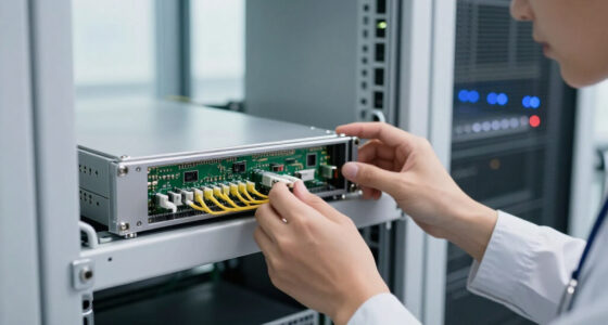
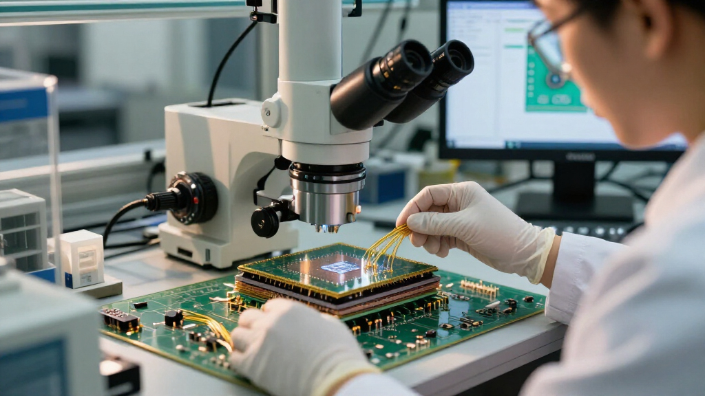
The package’s layers serve different purposes. A substrate provides connections to the module and circuit board; a silicon interposer carries dense connections among compute dies and memory; and liquid-cooling plates sit above the components. HBM is made by stacking DRAM chips and connecting them with through-silicon vias, or TSVs. This places memory close to the compute dies and supports more bandwidth than a conventional board connection can provide.
The source contrasts current designs from Nvidia and AMD. Nvidia’s Rubin GPU is described as using two reticle-limited compute dies, while AMD says its MI350-series GPU integrates eight vertically stacked accelerator complex dies and two I/O dies. AMD’s MI355X has eight stacks of 12-high memory, according to the explainer. These are not single-die chips: the components and the packaging that joins them work together as one accelerator.
Bandwidth figures cited in the article illustrate the growth in memory throughput: Nvidia lists 19.2 TB/s for Rubin, compared with 900 GB/s for the V100. The source says the comparison reflects different products and generations; it does not by itself establish how quickly a particular AI model will run. Model performance also depends on the system and workload.
The explainer also connects package design to data-center scale. Nvidia’s GB200 and GB300 NVL72 rack designs contain 72 GPUs and 36 CPUs, arranged across compute and switch trays. Nvidia’s documentation describes coolant flowing through cold plates attached to CPUs and GPUs. The article says the GB200 NVL72 rack is specified for 120 kilowatts of cooling capacity.
Memory and Packaging Limit Supply
For AI operators, more compute on paper does not automatically translate into more usable capacity. The processor needs a steady flow of data, so memory bandwidth can limit performance when models and workloads demand more than the memory system can supply. HBM stacks address that need by placing memory close to the compute dies and providing many connections through the package.
The same design creates a manufacturing challenge. Large interposers and complex die stacks require specialized production and assembly. The source identifies advanced packaging as a bottleneck, alongside memory availability. If either is constrained, accelerator supply can remain tight even when demand for AI computing is high. That matters to organizations planning data-center capacity, since rack-scale systems also require substantial power and liquid cooling.
SK hynix expects demand to exceed supply through 2030, according to the explainer’s account of the company’s outlook. That is a company forecast, not a guarantee of future shortages or prices. It signals that memory supply remains a planning concern, while the actual availability and cost of complete systems will depend on production, customer demand and other parts of the supply chain.
Popular right now

Dyson V8 Cyclone Cordless Vacuum

KitchenAid 5.5-Quart Bowl-Lift Stand Mixer, Porcelain White

Samsung 55-Inch M70H Series 4K HDR Mini-LED Smart TV with HDMI Cable and 12-Month CPS Warranty
As an affiliate, we earn on qualifying purchases.
From Interposer to Rack
The manufacturing limits begin with size. A lithography reticle is the largest area a scanner can print in one exposure. TSMC says its CoWoS-S packaging can accommodate an interposer up to about 2,700 square millimeters, or 3.3 times reticle size. For larger packages, CoWoS-L joins smaller silicon bridges in a carrier layer. The source says TSMC’s CEO reported on October 15, 2026, that the company was in real-world production of five-reticle-size packaging and was working on larger formats.
Memory stacks are also becoming taller while individual DRAM layers become thinner. JEDEC’s HBM4 standard, published in April 2025, allows stacks of four, eight, 12 or 16 layers and up to 64 GB per stack. Those specifications describe what the standard permits; they do not mean every accelerator uses the maximum stack height or capacity.
At rack level, the components require more than a package and a power connection. Nvidia’s cited NVL72 configuration combines GPU and CPU trays with NVLink switch trays, management switches and power shelves. The source describes an open rack measuring 600 millimeters wide, 1,068 millimeters deep and 2,236 millimeters high. Its dimensions and component count show why accelerator availability is tied to the broader infrastructure required to install and cool the systems.
Supply Outlook Has Limits
The source does not give a complete, independent measure of current HBM or advanced-packaging supply, nor does it quantify how much each constraint affects accelerator output. SK hynix’s forecast that demand will exceed supply through 2030 is a company outlook; the article does not provide its assumptions or a year-by-year estimate.
Some design and performance details also remain limited. The source says companies do not publish the dimensions of individual dies, packages or HBM stacks in millimeters, and its models use schematic sizes. Product specifications and packaging roadmaps may change. The cited bandwidth numbers compare products from different generations and do not establish performance for every model, server or workload.
The article provides rack configurations and cooling figures for named systems, but it does not compare their total operating costs, power efficiency or real-world availability. It also does not establish how much of the reported packaging capacity is allocated to each AI accelerator maker.
Watch Packaging and Memory Output
The next indicators are whether memory suppliers expand HBM production and whether packaging makers can increase output for larger interposers and stacked-die designs. Company updates on capacity and product availability will help clarify how the cited supply outlook is developing. Buyers will also need to track complete-system delivery, since GPU packages require compatible servers, rack infrastructure and cooling.
For newer accelerator generations, published specifications should show how compute dies, HBM capacity and bandwidth change together. Until manufacturers report more detailed production and shipment figures, the exact contribution of memory and packaging constraints to system availability remains uncertain.
Key Questions
Why do AI accelerators use HBM?
HBM puts stacked DRAM close to compute dies and uses vertical connections called TSVs. The design supports high memory bandwidth, helping supply data to processors running demanding AI workloads.
What does a silicon interposer do?
A silicon interposer connects compute dies and memory stacks with dense wiring. It can carry many more connections within a package than a conventional circuit board connection.
Why can advanced packaging limit AI chip supply?
Large interposers and stacked components require specialized production and assembly. If packaging capacity is constrained, manufacturers may not be able to turn available dies and memory into as many complete accelerators.
Does a higher bandwidth figure guarantee faster AI systems?
No. Bandwidth is one factor in performance. Results also depend on the accelerator, server design, workload and software, so figures for different product generations are not direct guarantees of model speed.
What did SK hynix say about memory supply?
The source reports that SK hynix expects memory demand to exceed supply through 2030. That is the company’s forecast; the source does not provide a detailed annual supply estimate or establish future prices.
Source: ThorstenMeyerAI.com